Allyanz Electronics, Semiconductors, Integrated Modules, Displays. Manufacturers Representative & Distributor Australia, NZ & South East Asia. Tel: +61.3.9759 5949
Lattice iCE40 Ultra / UltraLite / UltraPlus
Size & power matter.
World’s smallest, lowest power, most integrated mobile FPGAs.
- World’s most popular mobile FPGA – The iCE40 family has been designed into multiple generations of high-volume mobile and IoT edge applications, shipping at over 1 Million units per day.
- Reduce power, without compromising features – Extend battery life, while adding functionality to your designs using a unique, low-power FPGA architecture with integrated DSPs and large blocks of RAM.
- Free your designs from space constraints – Ultra small 1.4 mm x 1.4 mm x 0.45 mm WLCSP package removes all barriers to innovation and customization. Available in advanced 0.35 mm pitch package.
Features
- Ranging from 640 LUTs to 5,280 LUTs
- Key IP for sensor buffering, display driver, IR, barcode, voice, USB Type-C, user ID, and more…
- Flexible I/Os for signal type and positioning interfaces enable optimized layout, with more distributed heterogeneous processing architecture (DHP) 48 MHz high performance oscillator, 10 KHz low power Oscillator
- Three 24 mA and one 500 mA current drive outputs used for RGB LEDs or IR LEDs
- Up to 26 I/Os for customized interfaces
- Up to 1.1 Mbit of single port RAM
- Up to 8x DSP blocks to support 16 x 16 Multiply
- I/O Support for I3X, MIPI D-PHY & more..
Please contact Allyanz today for further details and support, including samples or evaluation boards.
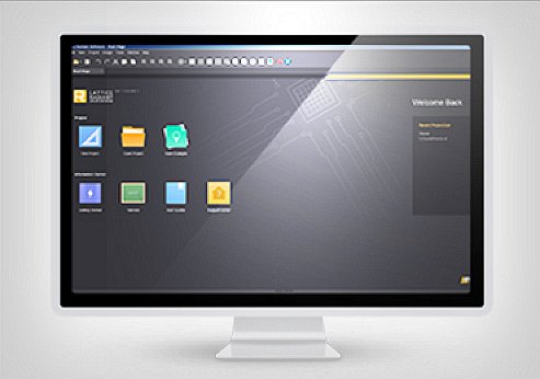
Lattice Radiant Software

- Full Featured Tool Suite for Edge Applications – Lattice Radiant software, supporting iCE40 UltraPlus, offers all the best in class tools and features to help users develop their Edge applications effectively and efficiently.
- Predictable Design Convergence – Achieving fast and predictable design convergence requires the design software to have a complete unified environment. Lattice Radiant software addresses this need by enabling a unified design database, design constraints flow, and timing analysis throughout the flow.
- Unparalleled Ease of Use – To provide the best user experience, Lattice Radiant software brings the ease of use of an FPGA design software to a whole new level with a redesigned user interface.
http://files.latticesemi.com/finalVids/Choon_Radiant_EN.mp4
Features
- Industry standard IEEE 1735 IP Encryption and Synopsys Design Constraint (SDC) for maximum interoperability.
- Ease of design navigation and debugging enabled by integrated tools set environment.
- Simple “One Click” design implementation execution enabled by a new Process Toolbar.
- Complete close-loop physical to logical design implementation cross probing.
- Common message viewing console with effective classification and filtering capabilities.
Getting Started
- Download Software Below – Windows / Linux
- Install: follow the installation guide, found in Documents section below.
- License: determine which license type you need, then request it on our licensing page via the button below.
Please contact Allyanz today for further details and support on Lattice Radiant.
Lattice Semiconductor Closes Acquisition of Silicon Image
Forms Global Leader in Smart Connectivity Solutions.

Lattice Semiconductor Corporation (NASDAQ:LSCC), a leading provider of
programmable connectivity solutions, has completed acquisition of
Silicon Image, Inc., a leading provider of wired and wireless
connectivity solutions.
For the first time in the semiconductor industry, a single company now combines the design flexibility and time to market benefits of FPGAs, with the highly integrated, function and cost optimization benefits of ASSPs. The all-cash acquisition, valued at approximately $606.6 million (or approximately $466.6 million on an enterprise value basis), is expected to be immediately accretive to EPS on a non-GAAP basis.
Darin G. Billerbeck, Lattice Semiconductor’s President and Chief Executive Officer, said, “Today marks an exciting day for Lattice, as we close our transformative acquisition of Silicon Image. We have significantly expanded our Company’s capabilities, with the addition of MHL, HDMI and 60 GHz Intellectual Property, enhanced our business prospects and financial profile, and further diversified our global customer base. We will move forward quickly in order to realize the compelling revenue and operating synergies created by our increased economies of scale. Our team has put in place a well thought through, comprehensive consolidation plan for an efficient integration and the achievement of our targeted cost synergies. We plan to work relentlessly over the coming years to rapidly deleverage through our increased free cash flow, and to achieve the full benefits of this major acquisition for our customers, shareholders and employees.”
For more information on how we can support your design with Smart Connectivity Solutions, please contact Allyanz.
LATTICE ECP5 FPGA Family for High-Volume Small-Cell, Microserver, Broadband Access & Video Applications

Lattice Breaks the Rules with ECP5 FPGA Family for High-Volume Small-Cell, Microserver, Broadband Access & Video Applications
New family combines 40% lower-cost, 30% lower power and 2X functional density in the smallest package to meet the unique needs of fast growing high-volume markets
Lattice Semiconductor Corp. (NASDAQ: LSCC) has announced availability of its ECP5(TM) family for small-cell, micro-server, broadband access, industrial video and other high-volume applications, where lowest-possible cost, lowest-possible-power, and smallest-possible form-factor are crucial.
The ECP5 Family ‘breaks the rules’ of conventional FPGA approaches to deliver a SERDES-based solution for designers to rapidly add features and functions to complement those delivered by ASICs and ASSPs, reducing development risk and quickly overcoming time-to-market challenges.
Key Features and Benefits
Cost Optimized Architecture
- Focused on providing best value below 100K LUTs.
- Smart ball depopulation simplifies package integration with existing PCB technology.
- Double Data Rate capability improves DSP block utilization.
Small Packages with High Functional Density
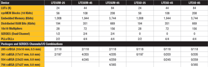
- 85K LUTs in 10×10 mm, 0.5 mm pitch package with SERDES.
Low Power Consumption
- Single channel SERDES functions below 0.25W.
- Quad channel SERDES functions below 0.5W.
Lattice has optimized the ECP5 family’s architecture with the goal of delivering best value below 100k LUTs for performing critical functions as a companion chip to ASICs and ASSPs. Achieving 40% lower cost than competing solutions, optimizations include small LUT4 based logic slices with enhanced routing architecture, dual-channel SERDES to save silicon real estate, and enhanced DSP blocks for up to 4x resource improvements.
“The ECP5 family breaks the rule that FPGAs should be the highest density, power hungry and expensive,” said Lattice Semiconductor President and CEO Darin Billerbeck. “Lattice’s newest family serves to provide customers with an ASIC/ASSP companion chip as the quickest path for removing development obstacles at a time when mobility and mobile infrastructure are driving the need for small size and low power in practically every facet of the electronics industry.”
The global deployment of next generation telecommunications systems is driving small-cells into high-volume, access and networking equipment is becoming commoditized and video display technologies continue to advance. For each of these applications, FPGA capabilities in a tiny, low-cost form-factor burning just milli-watts of power can eliminate many roadblocks for pursuing opportunities that would otherwise be ruled out due to ASIC development costs and schedules, or ASSP inflexibility and availability.
In wireless and wireline applications, the ECP5 family delivers an FPGA solution for enabling implementation of data path bridging and interfacing in a small, low-cost package. ECP5 FPGAs provide the flexible connectivity required in outdoor small-cells, at extremely low-cost. They can also enable a smart SFP (small form-factor pluggable) transceiver solution for broadband access equipment, including integrated operation and maintenance, in a compact 10mm x 10mm package.
Outside of communications, ECP5 devices offer low cost, low power PCI Express side-band connectivity for micro-servers.
For industrial video cameras, ECP5 FPGAs can implement the entire image processing functionality in a device that consumes under 2W.
The ECP5 family is the only FPGA portfolio in the industry that enables 85k LUTs and SERDES in 10mm x 10mm packages, amounting to 2X the functional density of competing solutions. Smart ball depopulation further simplifies package integration with existing PCB technology and reducing overall system cost.
Enhancements leading to 30% lower total power than other FPGA solutions include stand-by mode operation of the individual blocks including SERDES, dynamic IO bank controllers and reduced operating voltage. This enables single channel 3.25Gpbs SERDES functions starting below 0.25W, and quad channel SERDES functions starting below 0.5W for supporting a broad range of interface standards, including DDR3, LPDDR3, XGMII and 7:1 LVDS, PCI Express, Ethernet (XAUI, GbE, SGMII) and CPRI.
The ECP5 FPGA family is supported today in the Lattice Diamond(R) Software Tool.
Devices are available immediately with production-qualification scheduled for August 2014.
For more details, or to organise samples for your next design, please contact Allyanz.
New MachXO3 FPGA Family from Lattice Semiconductors
Most Advanced, Lowest Cost per I/O Programmable Bridging and I/O Expansion Solution
Leveraging 40nm technology, the MachXO3 FPGA family from Lattice Semiconductors delivers a new set of capabilities that enable system engineers to do even more in a smaller footprint.
- High-Speed SERDES – Support for 3.125Gbps transceivers – making high-bandwidth serial truly affordable
- Built-in Interfaces – Hard MIPI, PCIe, and GbE IP cores simplify interfacing and bridging
- High Performance, Lowest Power – 150MHz fabric speed while consuming uW static and mW active power
- The Industry’s Most Complete MIPI Based Solution – Achieve high bandwidth programmable bridging for consumer applications such as 4Kx2K video, 40MPixel image sensor interfaces
- Integrated Hard PCIe, and GbE IP – Enables high-speed control interfaces, as well as high-bandwidth data bridges in the lowest power, lowest cost ultra-low density FPGAs
- Hot-swap I/O – Eliminates system downtime in communication, storage and compute applications by enabling components to be swapped out without taking the rest of the system down
- On-chip Regulators – Single supply solution that leverages on-chip regulators to simplify design
- Innovative Packaging – Wirebond, flipchip, and Wafer Level Chip Scale Packaging technology leveraged for high I/O count in the right pitch to minimize package size
MachXO3 FPGA are available from Lattice in Automotive, Industrial and Commercial Temperature ranges.
Please contact Allyanz today to discuss further details, including Early Access Program for MachXO3 FPGAs.