Allyanz Electronics, Semiconductors, Integrated Modules, Displays. Manufacturers Representative & Distributor Australia, NZ & South East Asia. Tel: +61.3.9759 5949
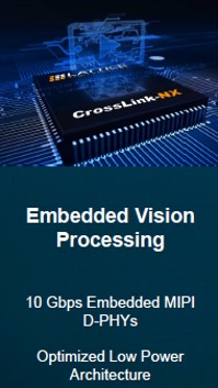
Lattice Introduces Industry’s First Small Embedded Vision FPGA with Integrated USB
Extends small, low-power FPGA portfolio with first-in-class FPGA featuring hardened USB for AI & embedded vision applications
Lattice Semiconductor (NASDAQ: LSCC), the low power programmable leader, introduces the Lattice CrossLinkU™-NX FPGA family, the industry’s first FPGAs with integrated USB device functionality in their class.
CrossLinkU-NX FPGAs help accelerate USB-equipped system designs and simplify thermal management through a combination of a hardened USB controller and physical layer (PHY), a unique low power standby mode, and a complete set of reference designs.
Extending Lattice’s embedded vision sensor bridging leadership with USB host interfaces, CrossLinkU-NX FPGAs are designed to meet growing customer needs to simplify USB-based design for applications across the Computing, Industrial, Automotive, and Consumer markets.
“Reducing power consumption, total cost of ownership, and design footprint are critical for expanding the potential of AI and vision applications,” said Dan Mansur, Vice President, Product Marketing, Lattice Semiconductor. “Lattice CrossLinkU-NX FPGAs are optimized to address these demands by integrating our low power, small form factor leadership with the popular USB connectivity interface to help designers extend battery life and simplify system design.”
Built on the award-winning Lattice Nexus™ platform, key features and performance highlights of the new low power Lattice CrossLinkU-NX FPGAs include:
* Vision Processing FPGAs with USB
- Featuring hardened USB 2.0 up to 480 Mbps and USB 3.2 up to 5 Gbps
- Reducing total cost of ownership and area needed for discrete PHY components
- Reducing FPGA fabric resources required for USB device controller
* Low Power Standby Mode with Always-On (AON)
- Extending battery life and simplifying system thermal management
- Optimizing power consumption in a typical embedded vision application
* Complete Set of Reference Designs
- Offering a Lattice Propel™ template, host driver, and example host utilities for USB to I/O bridging and MIPI CSI-2 to USB bridging applications to accelerate USB device implementation on the FPGA
CrossLinkU-NX FPGAs are available today & are supported with the latest release of Lattice Radiant® design software.
For more details or if you would like to discuss your design needs, please contact Allyanz.
NEW Lattice Avant FPGAs
Taking Low Power to New Heights
The Lattice Avant™ 16nm FinFET platform is the foundation for industry leading low-power and small form factor mid-range FPGA families. The platform features class leading 25 Gb/s SERDES, hardened PCI Express and external memory PHY interfaces, with high DSP counts for the latest AI/ML and computer vision algorithms.
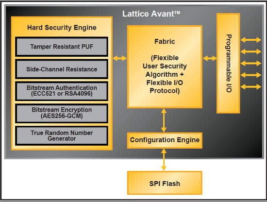
The Avant platform offers best in class reliability and security to suit a wide range of applications.
First to be released is the Avant™-E family of mid-range FPGAs, that are the first products built using the 16nm FinFET Avant platform.
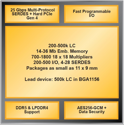
This platform has been optimized to deliver the lowest power, smallest form factor, and highest performance FPGA devices in their class. The Avant-E family delivers the highest DSP and embedded memory to logic ratio for mid-range FGPAs, enabling intelligence at the edge for applications in automotive, communications, compute, and industrial market segments.
- High Performance, Compact, and low power – High logic capacity from 200k to 500k LCs, smallest 11 x 9 mm package option, and up to 2.5x lower power than competition
- Fast External Memory Support – LPDDR4/DDR4 at 1800 Mbps
- Efficient Edge AI Processing – Up to 7200 INT8 multipliers and 36 Mb embedded memory enable more efficient implementation of AI/ML algorithms
Lattice will introduce additional Avant families to leverage the full capabilities of the platform. Click here to be notified as new devices become available.
To learn more about Lattice Avant FPGAs, please contact Allyanz or visit our Resource Centre.
Lattice Launches New CertusPro-NX
Lattice CertusPro-NX General Purpose FPGA
Lattice is excited to announce our new, advanced general purpose FPGA family, Lattice CertusPro™-NX. The company’s fourth FPGA family based on the Lattice Nexus™ development platform, CertusPro-NX FPGAs deliver best-in-class system bandwidth, industry-leading power efficiency, and support new protocols and advanced standards for next-gen applications in the communications, compute, industrial, automotive, and consumer markets.
CertusPro-NX FPGAs are designed to enable customer innovation around applications including data co-processing in intelligent systems, high-bandwidth signal bridging in 5G communications infrastructure, and sensor interface bridging in ADAS systems.
Class-leading power efficiency – By leveraging Lattice’s innovations in FPGA fabric architecture and a low power FD-SOI manufacturing process, CertusPro-NX devices deliver exceptional performance while consuming up to four times less power than competing FPGAs of a similar class.
Best-in-class system bandwidth – With support for up to eight programmable SERDES lanes capable of speeds up to 10.3 Gbps, CertusPro-NX FPGAs deliver the highest system bandwidth in their class to enable popular communication and display interfaces like 10 Gigabit Ethernet, PCI Express, SLVS-EC, CoaXPress, and DisplayPort.
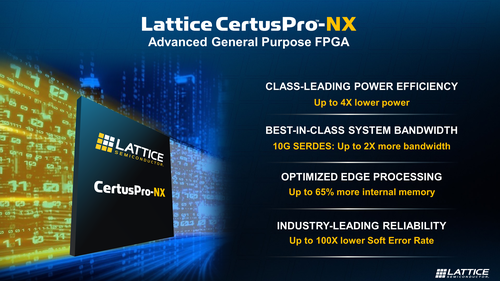
Optimized Edge processing – To meet demand for robust data co-processing in Edge AI and ML applications, CertusPro-NX FPGAs feature up to 65 percent more available on-chip memory than other similar FPGAs. CertusPro-NX devices are the only low power FPGAs currently supporting the LPDDR4 DRAM memory standard which is preferred due to its projected long-term availability.
High logic density – With support for up to 100k logic cells, CertusPro-NX FPGAs currently offer the highest logic density of any Nexus-based FPGA.
Industry-leading reliability – Mission-critical automotive, industrial, and communications applications must deliver high availability to enable predictable performance and keep users safe. Thanks to innovations in the Lattice Nexus platform, CertusPro-NX devices are up to 100 times more resistant to soft errors.
Smallest-in-class form factor – With a design footprint of 81 mm2, CertusPro-NX FPGAs are up to 6.5 times smaller than competing devices. Small form factor is a key design consideration for developers of industrial cameras or the SFP modules used in communication systems.
To learn more about CertusPro-NX FPGAs, please contact Allyanz or visit our Resource Centre.
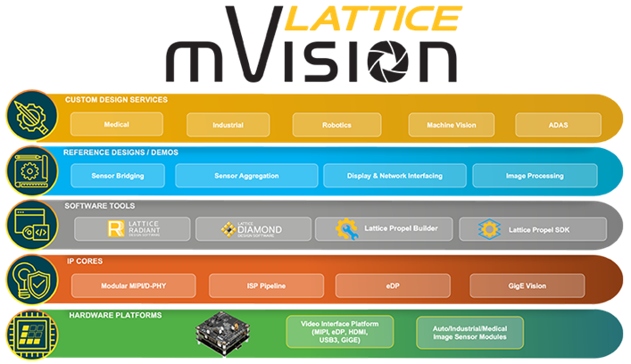
Lattice mVision™ Solutions Stack 2.0 For Embedded Vision Systems
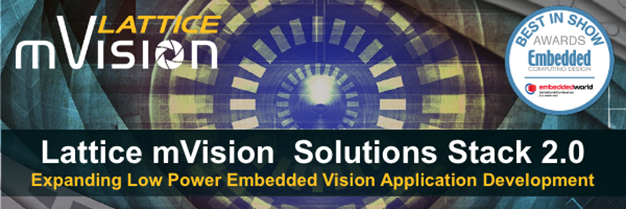
Lattice mVision™ Solutions Stack 2.0
Lattice has launched a new, enhanced version of the award-winning mVision™ solutions stack, mVision 2.0. With new features and expanded end-market application support, mVision 2.0 makes it easier than ever for embedded vision system designers to evaluate, develop, and deploy FPGA-based embedded vision applications, such as machine vision, robotics, ADAS, video surveillance, and drones.
Lattice mVision 2.0 Highlights:
- Added new development boards supporting popular image sensors for industrial and medical applications – including the Sony IMX464, Sony IMX568, and the AR0344CS from ON Semiconductor
- Support for Lattice Propel Design Environment – our easy-to-use software design environment for accelerating embedded processor-based development on Lattice FPGAs
- New Lattice Image Signal Processing (ISP) Reference Design
Please Contact Allyanz today to find out how Lattice mVision can help enhance your next embedded vision design!
Lattice Certus-NX Redefines Low Power, High I/O Count FPGAs
Looking for an FPGA that delivers greater I/O density and lower power in a significantly smaller package? Check out Lattice’s new Certus™-NX family of FPGAs. Leveraging the tremendous advantages of Lattice’s new Nexus platform – the industry’s first low power FPGA platform to use a 28-nm FD-SOI process technology – Certus-NX offers industrial and automotive designers best-in-class power savings, up to a 3x smaller form factor, higher reliability, and instant-on performance.

And to help designers meet rapidly changing connectivity and performance needs, the Certus-NX adds PCIe and Ethernet chip-to-chip connectivity.
Features include:
- Up to 39K logic cells, 2.9 Mb embedded memory, 56 18 x 18 multipliers, 192 programmable I/O, one lane of 5 Gbps PCIe, two lanes of 1.25 Gbps SGMII, two ADCs (each 12-bit, 1 MSPS).
- Packages as small as 6×6 mm, and in ball-pitch options of 0.5 and 0.8 mm.
- Power modes – User selectable Low Power vs. High Performance modes, enabled by FD-SOI programmable back-bias.
- Design security – ECDSA bitstream authentication, coupled with robust AES-256 encryption.
- Instant-on configuration – I/O configures in 3 ms, and full-device as fast as 8 ms.
Additionally, Lattice released version 2.1 of the Radiant design software, which includes support for Certus-NX and SystemVerilog to make it easier than ever for developers to build applications based on the latest FPGA technology.
For more information, evaluation boards or samples please contact Allyanz.