Allyanz Electronics, Semiconductors, Integrated Modules, Displays. Manufacturers Representative & Distributor Australia, NZ & South East Asia. Tel: +61.3.9759 5949
Lattice Semiconductor Closes Acquisition of Silicon Image
Forms Global Leader in Smart Connectivity Solutions.

Lattice Semiconductor Corporation (NASDAQ:LSCC), a leading provider of
programmable connectivity solutions, has completed acquisition of
Silicon Image, Inc., a leading provider of wired and wireless
connectivity solutions.
For the first time in the semiconductor industry, a single company now combines the design flexibility and time to market benefits of FPGAs, with the highly integrated, function and cost optimization benefits of ASSPs. The all-cash acquisition, valued at approximately $606.6 million (or approximately $466.6 million on an enterprise value basis), is expected to be immediately accretive to EPS on a non-GAAP basis.
Darin G. Billerbeck, Lattice Semiconductor’s President and Chief Executive Officer, said, “Today marks an exciting day for Lattice, as we close our transformative acquisition of Silicon Image. We have significantly expanded our Company’s capabilities, with the addition of MHL, HDMI and 60 GHz Intellectual Property, enhanced our business prospects and financial profile, and further diversified our global customer base. We will move forward quickly in order to realize the compelling revenue and operating synergies created by our increased economies of scale. Our team has put in place a well thought through, comprehensive consolidation plan for an efficient integration and the achievement of our targeted cost synergies. We plan to work relentlessly over the coming years to rapidly deleverage through our increased free cash flow, and to achieve the full benefits of this major acquisition for our customers, shareholders and employees.”
For more information on how we can support your design with Smart Connectivity Solutions, please contact Allyanz.
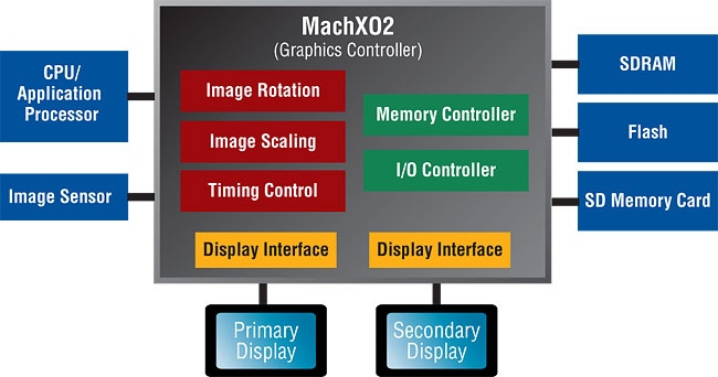
Lattice MachXO2 PLD – Processor I/O Expansion with MachXO2 Cuts Cost and Reduces Power
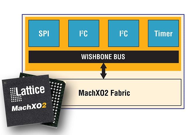
Using the Lattice MachXO2 PLD’s hardened block functions you can easily add extra functions and more I/Os to a low pin count/low cost MCU based design. This reduces component cost, saves board space and saves power vs. using a higher pin count MCU. Also, the MachXO2 carries no overhead since it needs no configuration device.
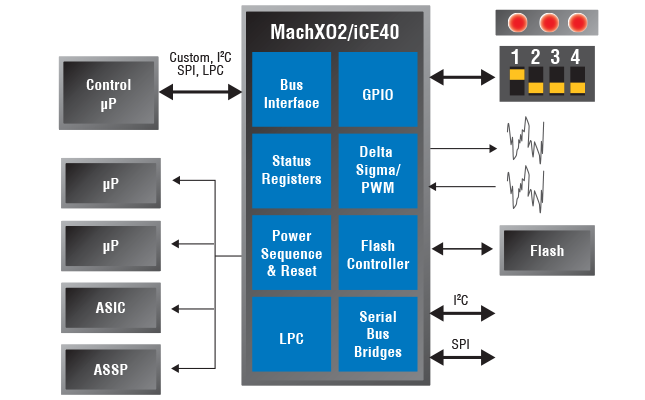
- Discover how the hardened dual I2C, SPI, and Timer/Counter functions augment the flexible I/Os and logic blocks in the MachXO2 to efficiently support MCU-based designs.
- See how a sensor monitoring solution example takes full advantage of the MachXO2 I/O expansion capabilities.
- Watch the 7-minute video to better understand how the MachXO2 efficiently integrates system functionality and how easy it is to get started with free design tools, IP trials and reference designs.
Visit the “Lattice MachXO2 I/O Expansion” web page to explore the full capabilities of the MachXO2 as an MCU I/O expansion device, or please
contact Allyanz todayfor more details.
Lattice Semiconductor Announces Serial Image Sensor Bridge Support For Sony IMX136/104
Lattice Semiconductor Corporation (NASDAQ: LSCC), has announced the release of a serial sub-LVDS bridge design to support the Sony IMX136 and IMX104 image sensors. The serial sub-LVDS format is expected to become Sony’s primary image sensor interface for embedded/industrial users.
This new image sensor bridge design utilizes the low cost, low power Lattice MachXO2(tm) PLD (programmable logic device) to interface to the serial sub-LVDS bus of the Sony IMX136 or IMX104 image sensor. Applications that can benefit from this design include Surveillance cameras, Video conferencing and Industrial cameras.
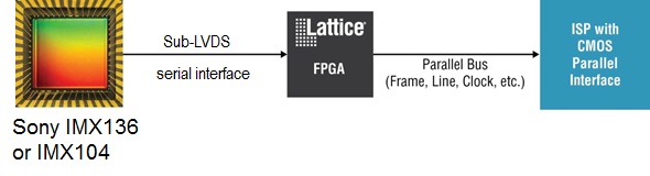
This image sensor bridge design allows an ISP (Image Signal Processor) with a CMOS parallel interface bus to connect to the Sony IMX136 or IMX104. The Lattice MachXO2-1200 device interfaces directly to the sub-LVDS I/Os and no external discrete components are required. The image sensor bridge application can support 1080P60 resolution with a 12-bit ISP interface.
If customers desire the full 1080P120 capability of the Sony IMX136 or IMX104, then the design code in the MachXO2 device can be modified easily to accommodate this. The image sensor bridge design is available now for download, and the MachXO2-1200 is in full production.
Key features:
- Complete Reference Designs in MachXO2-1200 or XP2-5
- Designed to Emulate Parallel Sensor Output Bus Width of 10 or 12 Bits
- Serial sub-LVDS interface to CMOS SDR data
- Legacy sub-LVDS parallel DDR to CMOS SDR also available
- Tested with Sony IMX036 and TI DM812X at 1080p60
- Converts the Sub-LVDS Sync Commands to Line Valid and Frame Valid Signals
- Bridge Device Offered in Space-saving 8×8 mm 132-Ball csBGA. TQFP Packages Also Available.
- Requires No External PROM
- Parallel Interface can be Configured for 1.8V, 2.5V or 3.3V LVCMOS Levels
To obtain the Sony IMX136 or IMX104 serial image sensor bridge design files, visit http://www.latticesemi.com/products/intellectualproperty/referencedesigns/sonyimx036sensorwithsublv.cfm , or please contact Allyanz.
Lattice Announces Production Release Of iCE40 “Los Angeles” LP-Series And HX-Series mobileFPGA Device Families
Two New iCEblink40 Development Kits Enable Access to Production-Qualified, Non-volatile 40nm Programmable Technology
Lattice Semiconductor Corporation (NASDAQ: LSCC) has announced that eight devices of its iCE40TM “Los Angeles” mobileFPGATM family have been fully qualified and released into volume production. The LP640, LP1K, LP4K and LP8K devices of the iCE40 low power LP-Series, and the HX640, HX1K, HX4K and HX8K devices of the higher performance iCE40 HX-Series, have been production released with 17 different device/package combinations.

The iCE40 mobileFPGA family, fabricated on non-volatile 40nm technology, follows the very successful 65nm iCE65TM family that has already been adopted by large consumer electronics OEMs who have taken advantage of its flexibility, low power, low cost and small footprint to quickly create new and innovative consumer products within ever shrinking development cycles.
Easy to Use Development Kits
With two new iCEblinkTM Development Kits, engineers can easily evaluate and adopt non-volatile iCE40 technology. The iCEblink40-HX (higher performance) Development Kit comes with an iCE40HX1K-VQ100 device and the iCEblink40-LP (low power) Development Kit comes with an iCE40LP1K-QN84 device. Both devices offer 1280 look up tables of logic, 64K bits of on-chip memory, and 67 user I/O. The USB-powered iCEblink40 Development Kits include features such as 1Mbit of SPI Flash memory, capacitive touch buttons, LEDs and access to all user I/O.
The iCEblink40 Development Kits are available for immediate purchase on Lattice’s website. For more information on the iCEblink40HX Development Kits, or the ultra low power consuming iCE40 mobileFPGAs, visit www.latticesemi.com/iCEblink40-HX1K, or please contact Allyanz.
LATTICE MachXO2 PLD Family Sets New Standards For Low Cost, Low Power Designs
— Over 100X Power Reduction, Up to 30% Lower Cost,
Highlight New Benefits for Low-density PLD Designers —
Lattice Semiconductor Corporation (NASDAQ: LSCC) has unveiled its new MachXO2TM PLD family, which offers designers of low-density PLDs an unprecedented mix of low cost, low power and high system integration in a single device. Built on a low power 65-nm process featuring embedded Flash technology, theMachXO2 family delivers a 3X increase in logic density, a 10X increase in embedded memory, more than a 100X reduction in static power and up to 30% lower cost compared to the MachXOTM PLD family. In addition, several popular functions used in low-density PLD applications, such as User Flash Memory (UFM), I2C, SPI and timer/counter, have been hardened into the MachXO2 devices, providing designers a “Do-it-All-PLD” for high volume, cost sensitive designs.
“Through the use of 65-nm embedded Flash technology, we have reduced costs and increased functionality for our traditional customers in the computing, industrial and telecommunication infrastructure markets, while dramatically reducing power consumption for designers of consumer equipment,” said Gordon Hands, Director of Marketing for Low Density and Mixed Signal Solutions. “Many early access customers are already evaluating and designing with MachXO2 devices in a broad range of applications.”
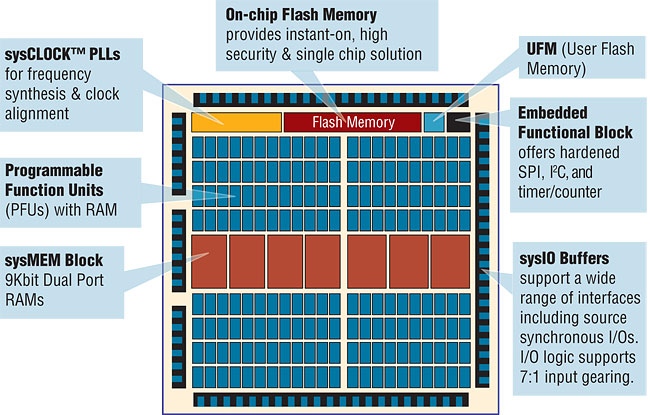
MachXO2 Block Diagram
Three Product Options For Maximum Flexibility
The MachXO2 family offers three options for maximum flexibility. MachXO2 ZE devices range from 256 to 7K look-up tables (LUTs), operate off a nominal 1.2V power supply, and support system performance up to 60MHz. With power specified as low as 19uW and packages as small as 2.5mmx2.5mm, the MachXO2 ZE devices are optimized for cost-sensitive, low power consumer design applications such as smart phones, GPS devices and PDAs.
MachXO2 HC devices range from 256 to 7K LUTs, operate off a nominal 3.3V or 2.5V power supply, and support system performance up to 150MHz. Offering up to 335 user I/O and a robust design solution (instant-on, non-volatile, input hysteresis and single-chip), these devices are ideal for control applications in end markets such as telecommunications infrastructure, computing, industrial and medical equipment.
MachXO2 HE devices range from 2K to 7K LUTs, operate off a nominal 1.2V power supply and support system performance up to 150MHz. These devices are optimized for power sensitive system applications.
Free Design Tools and Free Reference Designs Accelerate Development Time
Customers can start designing with MachXO2 devices today using Lattice DiamondTM v1.1 software, which can be downloaded for free from the Lattice website at
http://www.latticesemi.com/latticediamond/downloads/
Existing ispLEVERR software users have the option to use the free ispLEVER v8.1 SP1 Starter software, downloadable from the Lattice web site, with an installed control pack. Visit http://www.latticesemi.com/starter.
In order to enable quick and efficient design and deployment of commonly used functions in system and consumer applications, more than 20 reference designs using MachXO2 devices can be downloaded for free from the Lattice website at http://www.latticesemi.com/referencedesigns.
For more information, including pricing or availability on devices from the new MachXO2TM PLD family, please contact us.