Allyanz Electronics, Semiconductors, Integrated Modules, Displays. Manufacturers Representative & Distributor Australia, NZ & South East Asia. Tel: +61.3.9759 5949
Lattice MachXO2 PLD – Processor I/O Expansion with MachXO2 Cuts Cost and Reduces Power
Using the Lattice MachXO2 PLD’s hardened block functions you can easily add extra functions and more I/Os to a low pin count/low cost MCU based design. This reduces component cost, saves board space and saves power vs. using a higher pin count MCU. Also, the MachXO2 carries no overhead since it needs no configuration device.
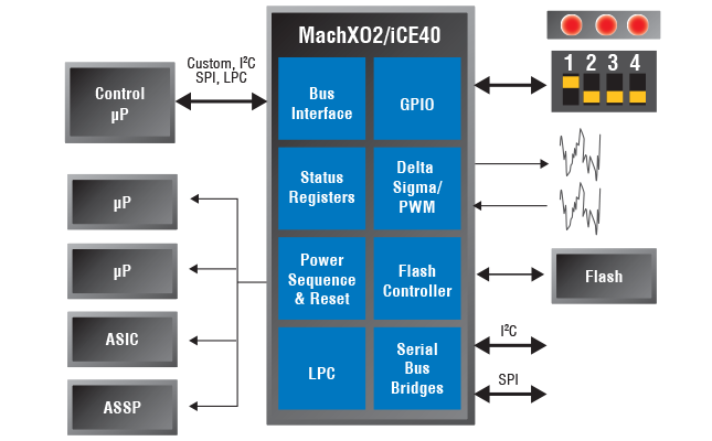
- Discover how the hardened dual I2C, SPI, and Timer/Counter functions augment the flexible I/Os and logic blocks in the MachXO2 to efficiently support MCU-based designs.
- See how a sensor monitoring solution example takes full advantage of the MachXO2 I/O expansion capabilities.
- Watch the 7-minute video to better understand how the MachXO2 efficiently integrates system functionality and how easy it is to get started with free design tools, IP trials and reference designs.
Visit the “Lattice MachXO2 I/O Expansion” web page to explore the full capabilities of the MachXO2 as an MCU I/O expansion device, or please
contact Allyanz todayfor more details.
Lattice FPGA Design Software Webinar Australia / New Zealand – September 8, 2010
Lattice Power 2 You! Webinar Series –
Australia / New Zealand – September 8, 2010

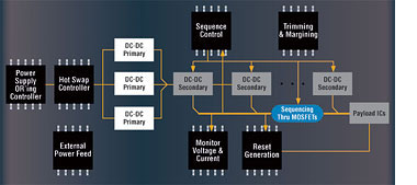
The Power 2 You! webinar helps you understand key design criteria for the power management functions shown in the below figure. In addition, the webinar will show you how to integrate them into a Power Manager II device. The resulting solution can be used across a wide range of applications and can be individually customized using Lattice’s PAC-Designer (R) software.
Attend this FREE Lattice Semiconductor seminar and you will walk away with in-depth technical knowledge of Lattice’s Power Manager Solutions.
All attendees receive a free copy of the Power 2 You! reference manual.
Learn How to Design
- Hot swap controllers
- Supply OR’ing controllers using MOSFETs
- Power feed through MOSFETs
- Power supply sequencing with and without MOSFETs
- Reliable monitoring voltages for fault and reset generation
- Trimming and margining of board-mounted supplies
For more information please contact us.
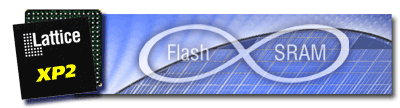
Single Chip, Non-Volatile LatticeXP2 FPGA
Lattice Semiconductor is now shipping industrial temperature, and automotive temperature (AEC-Q100, with PPAP support) qualified versions of its non-volatile LatticeXP2(TM) FPGAs in volume production quantities. Based on Lattice’s 90 nanometer hybrid flexiFLASH(TM) technology, the XP2 family’s volume production availability enables realization of design requirements in a multitude of industrial applications such as medical imaging, robotics, human machine interface (HMI) systems, motor control and industrial displays, as well as in the tightest form-factor automotive applications such as automotive camera modules, telematics systems, parking assistance systems and multimedia systems.
The non-volatile LatticeXP2 FPGA family is a compelling solution for designers who value single chip integration, impressive processing power in the smallest footprint, source synchronous interfaces, design security and low power consumption. The XP2 FPGAs unique benefits include low cost, small form factor Chip Scale 132 BGA packaging, and increased functionality such as embedded sysDSP(TM) blocks, pre-engineered source-synchronous I/O that supports 7:1 LVDS, DDR2 and high-speed ADCs/DACs.
Unlike traditional SRAM-based FPGAs, the LatticeXP2 device does not require an external boot memory for FPGA configuration, which enables a single-chip solution with the associated benefits of reduced board area and simplified system manufacture. The absence of an external boot device also eliminates the need for an external bit-stream at boot up and the possibility of bit-stream snooping, a major security concern with SRAM FPGAs. Additional security features prohibit bit-stream readback from the SRAM and Flash sections of the devices.
The LatticeXP2 design solution offers a unique set of features with broad appeal to a variety of markets, such as video security/ surveillance, LCD/display controllers, automotive systems, medical imaging, and industrial control systems, where processing power must be delivered with high integration in low-cost, small footprint packaging.
About flexiFLASH Architecture
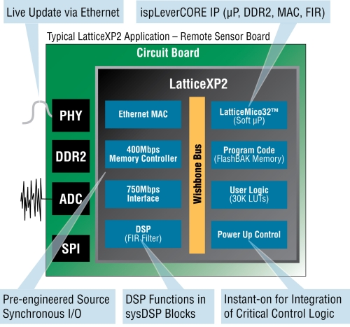
Flash memory blocks are embedded within XP2 FPGAs to store the device configuration, providing a true single chip solution. At power up or on user command, the data stored in the Flash memory is transferred into SRAM cells that control the configuration of the device. This transfer is done in a massively parallel fashion, enabling the device logic to be available in under 1mS, well ahead of the other devices in the system and much faster than SRAM-based FPGAs that use external boot PROMs, regardless of whether they are provisioned separately on-board or stacked in the same package. This instant-on capability is critical for many system functions such as power up sequencing, address decoding and reset logic.
For more details on the single chip, non-volatile LatticeXP2(TM) FPGAs, or development tools to support your design requirements, please contact us.
Lowest Power SERDES-capable FPGA in the industry
The LatticeECP3 family is the third generation high value FPGA from Lattice Semiconductor, which offers the industry’s lowest power consumption and price of any SERDES-capable FPGA device. The LatticeECP3 FPGA family offers multi-protocol 3.2G SERDES with XAUI jitter compliance, DDR3 memory interfaces, powerful DSP capabilities, high density on-chip memory and up to 149K LUTS, all with half the power consumption and half the price of competitive SERDES-capable FPGAs.
Features include:
- Low-power 65nm process with 4-input look-up table (LUT) fabric
- Logic densities from 17K to 149K LUTs
- Upto 6.8Mbits of Embedded Block RAM (EBR)
- 2 DLLs per device, 2 to 10 PLLs per device
- High Speed embedded SERDES
- Multiply, accumulate, addition and subtraction
- High performance Adder Trees and MMAC functionality
- 54-bit Cascadable Arithmetic Logic Unit
- 24 to 320 multipliers (18×18)
- Advanced configuration options
- Flexible I/O buffers
- Wide range of Package & User I/O options
For more information on the LatticeECP3 family of FPGAs, or development tools to support your design requirements, please contact us.