Allyanz Electronics, Semiconductors, Integrated Modules, Displays. Manufacturers Representative & Distributor Australia, NZ & South East Asia. Tel: +61.3.9759 5949
Lattice Certus-NX Redefines Low Power, High I/O Count FPGAs
Looking for an FPGA that delivers greater I/O density and lower power in a significantly smaller package? Check out Lattice’s new Certus™-NX family of FPGAs. Leveraging the tremendous advantages of Lattice’s new Nexus platform – the industry’s first low power FPGA platform to use a 28-nm FD-SOI process technology – Certus-NX offers industrial and automotive designers best-in-class power savings, up to a 3x smaller form factor, higher reliability, and instant-on performance.

And to help designers meet rapidly changing connectivity and performance needs, the Certus-NX adds PCIe and Ethernet chip-to-chip connectivity.
Features include:
- Up to 39K logic cells, 2.9 Mb embedded memory, 56 18 x 18 multipliers, 192 programmable I/O, one lane of 5 Gbps PCIe, two lanes of 1.25 Gbps SGMII, two ADCs (each 12-bit, 1 MSPS).
- Packages as small as 6×6 mm, and in ball-pitch options of 0.5 and 0.8 mm.
- Power modes – User selectable Low Power vs. High Performance modes, enabled by FD-SOI programmable back-bias.
- Design security – ECDSA bitstream authentication, coupled with robust AES-256 encryption.
- Instant-on configuration – I/O configures in 3 ms, and full-device as fast as 8 ms.
Additionally, Lattice released version 2.1 of the Radiant design software, which includes support for Certus-NX and SystemVerilog to make it easier than ever for developers to build applications based on the latest FPGA technology.
For more information, evaluation boards or samples please contact Allyanz.
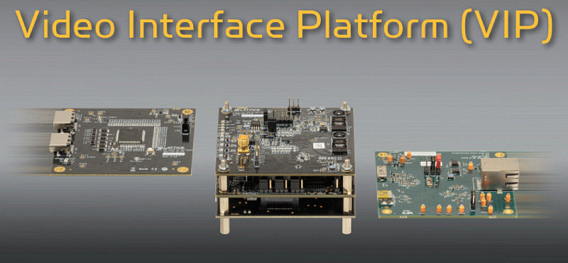
Lattice Extends Video Interface Platform to GigE/USB 3.0
Lattice Video Interface Platform GigE/USB 3.0
Need to quickly build embedded vision prototypes with Ethernet connectors running at Gigabit speeds?
Lattice’s latest I/O board for the Video Interface Platform (VIP) does just that. The new I/O board is the latest addition to Lattice’s highly modular platform.
By replacing cumbersome manual wiring with a unified connector, designers can quickly build plug-and-play solutions.
The new GigE/USB 3.0 I/O board allows developers to quickly and easily add network connectivity options to Lattice’s award-winning Embedded Vision Development Kit.
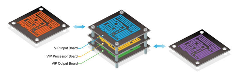
The kit combines a CrossLink mobile bridging input board, an optimised ECP5 image signal processing board, and high res HDMI VIP Input and Output boards into a ready-to-use platform.
The VIP platform also offers IP from 3rd party partners including commercial grade image signal processing and networking stacks, Helion Vision’s GigE Vision, multiple sensor board inputs, and DisplayPort IP from Bitec.
For more information on the Video Interface Platform from Lattice, please contact Allyanz today.
Lattice Announces Production Release Of iCE40 “Los Angeles” LP-Series And HX-Series mobileFPGA Device Families
Two New iCEblink40 Development Kits Enable Access to Production-Qualified, Non-volatile 40nm Programmable Technology
Lattice Semiconductor Corporation (NASDAQ: LSCC) has announced that eight devices of its iCE40TM “Los Angeles” mobileFPGATM family have been fully qualified and released into volume production. The LP640, LP1K, LP4K and LP8K devices of the iCE40 low power LP-Series, and the HX640, HX1K, HX4K and HX8K devices of the higher performance iCE40 HX-Series, have been production released with 17 different device/package combinations.

The iCE40 mobileFPGA family, fabricated on non-volatile 40nm technology, follows the very successful 65nm iCE65TM family that has already been adopted by large consumer electronics OEMs who have taken advantage of its flexibility, low power, low cost and small footprint to quickly create new and innovative consumer products within ever shrinking development cycles.
Easy to Use Development Kits
With two new iCEblinkTM Development Kits, engineers can easily evaluate and adopt non-volatile iCE40 technology. The iCEblink40-HX (higher performance) Development Kit comes with an iCE40HX1K-VQ100 device and the iCEblink40-LP (low power) Development Kit comes with an iCE40LP1K-QN84 device. Both devices offer 1280 look up tables of logic, 64K bits of on-chip memory, and 67 user I/O. The USB-powered iCEblink40 Development Kits include features such as 1Mbit of SPI Flash memory, capacitive touch buttons, LEDs and access to all user I/O.
The iCEblink40 Development Kits are available for immediate purchase on Lattice’s website. For more information on the iCEblink40HX Development Kits, or the ultra low power consuming iCE40 mobileFPGAs, visit www.latticesemi.com/iCEblink40-HX1K, or please contact Allyanz.
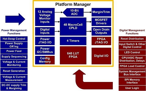
Platform Manager From Lattice Transforms Board Power & Digital Management
Programmable Devices Reduce Cost Up to 50%; Cut Weeks From Design Time; Monitor Power Supplies with 0.7% Accuracy
Lattice Semiconductor Corporation (NASDAQ: LSCC) has announced its third-generation mixed-signal devices, the Platform Managerâ„¢ family. The programmable Platform Manager devices are expected to simplify board management design significantly by integrating programmable analog and logic to support many common functions, such as power management, digital housekeeping and glue logic. By integrating these support functions, Platform Manager devices can not only reduce the cost of these functions compared to traditional approaches, but also can improve system reliability and provide a high degree of design flexibility that minimizes the risk of circuit board re-spins.
About the Platform Manager Family
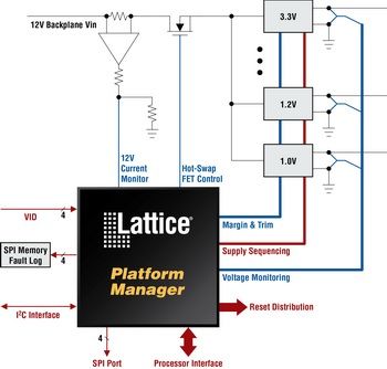
The Platform Manager product family consists of two devices, the LPTM10-1247 and LPTM10-12107. The LPTM10-1247 device can monitor 12 voltage rails and supports 47 digital I/O, while the LPTM10-12107 monitors up to 12 voltage rails and supports 107 digital I/O. Functionally, these devices include both a power management section and a digital board management section. The power management section consists of a programmable threshold, precision differential input comparator block with an accuracy of 0.7%, a 48-macrocell CPLD, programmable hardware timers, a10-bit analog to digital converter and a trim block for the trimming and margining of supplies. The digital board management section consists of a 640-LUT FPGA and programmable logic interface I/O.
For more details on the very popular Platform Manager devices from Lattice, please contact us.
Lattice Releases Development Platform for SERDES and Video Clock Distribution
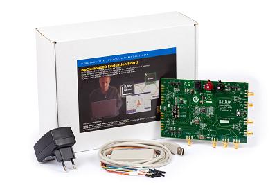
Lattice Semiconductor is now shipping its US$169 evaluation board for the ispClockTM 5400D programmable clock device.
The new board is an easy-to-use platform for evaluating and designing with the ispClock5400D differential clock distribution device. The evaluation board can be used by itself to review the performance and in-system programmability of the 5400D device, or as a companion board and clock source for LatticeECP3TM FPGA Serial Protocol or Video Protocol evaluation boards.
Typically, expensive oscillators with LVDS or LVPECL interfaces are used as a reference clock for FPGA SERDES interface applications. The ispClock5400D device provides ultra low-jitter differential clock outputs that can be used to drive both the general purpose clocks and the SERDES reference clocks for FPGAs, ASSPs and ASICs. The evaluation board demonstrates how to interface a low-cost CMOS interface oscillator to the ispClock5400D device to produce high quality clocks for XAUI applications or 270 MHz SDI video applications.
About ispClock Programmable Clock Devices
The ispClock5400D device family features in-system programmable differential clock distribution with fully programmable features that allow users to program in different frequencies based on dividers and PLL functions. Additional value is added with multiple differential I/O support for various standards while maintaining the low-jitter required for high performance systems. The ispClock5400D family supports differential output drivers for programmable differential input reference/feedback standards: LVDS, LVPECL, HSTL, SSTL and HCSL. Included on-chip are programmable termination and a clock A/B selection multiplexer, programmable time skew, programmable phase skew and various programmable output enable features. Through I2C the user has access to nearly all the programmable features of the ispClock5400D.
The ispClock5400D maintains extremely low-jitter:
- Ultra low cycle-to-cycle jitter (29ps p-p)
- Ultra low period jitter (2.5ps)
- Low output-to-output skew (<75ps)
About LatticeECP3 FPGAs
The low power, high value, third generation LatticeECP3 family offers the industry’s lowest power consumption and price of any SERDES-capable FPGA devices.The LatticeECP3 FPGA family offers multi-protocol 3.2G SERDES with XAUI jitter compliance, DDR3 memory interfaces, powerful DSP capabilities, high density on-chip memory and up to 149K LUTS, all with half the power consumption and half the price of competitive SERDES-capable FPGAs.
For more details on the low cost Evaluation board, ispClock5400D devices or ECP3 SERDES-capable FPGAs, please contact us.