Lattice Releases Development Platform for SERDES and Video Clock Distribution

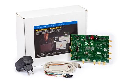
Lattice Semiconductor is now shipping its US$169 evaluation board for the ispClockTM 5400D programmable clock device.
The new board is an easy-to-use platform for evaluating and designing with the ispClock5400D differential clock distribution device. The evaluation board can be used by itself to review the performance and in-system programmability of the 5400D device, or as a companion board and clock source for LatticeECP3TM FPGA Serial Protocol or Video Protocol evaluation boards.
Typically, expensive oscillators with LVDS or LVPECL interfaces are used as a reference clock for FPGA SERDES interface applications. The ispClock5400D device provides ultra low-jitter differential clock outputs that can be used to drive both the general purpose clocks and the SERDES reference clocks for FPGAs, ASSPs and ASICs. The evaluation board demonstrates how to interface a low-cost CMOS interface oscillator to the ispClock5400D device to produce high quality clocks for XAUI applications or 270 MHz SDI video applications.
About ispClock Programmable Clock Devices
The ispClock5400D device family features in-system programmable differential clock distribution with fully programmable features that allow users to program in different frequencies based on dividers and PLL functions. Additional value is added with multiple differential I/O support for various standards while maintaining the low-jitter required for high performance systems. The ispClock5400D family supports differential output drivers for programmable differential input reference/feedback standards: LVDS, LVPECL, HSTL, SSTL and HCSL. Included on-chip are programmable termination and a clock A/B selection multiplexer, programmable time skew, programmable phase skew and various programmable output enable features. Through I2C the user has access to nearly all the programmable features of the ispClock5400D.
The ispClock5400D maintains extremely low-jitter:
- Ultra low cycle-to-cycle jitter (29ps p-p)
- Ultra low period jitter (2.5ps)
- Low output-to-output skew (<75ps)
About LatticeECP3 FPGAs
The low power, high value, third generation LatticeECP3 family offers the industry’s lowest power consumption and price of any SERDES-capable FPGA devices.The LatticeECP3 FPGA family offers multi-protocol 3.2G SERDES with XAUI jitter compliance, DDR3 memory interfaces, powerful DSP capabilities, high density on-chip memory and up to 149K LUTS, all with half the power consumption and half the price of competitive SERDES-capable FPGAs.
For more details on the low cost Evaluation board, ispClock5400D devices or ECP3 SERDES-capable FPGAs, please contact us.