Allyanz Electronics, Semiconductors, Integrated Modules, Displays. Manufacturers Representative & Distributor Australia, NZ & South East Asia. Tel: +61.3.9759 5949
Lattice MachXO2 PLD – Processor I/O Expansion with MachXO2 Cuts Cost and Reduces Power
Using the Lattice MachXO2 PLD’s hardened block functions you can easily add extra functions and more I/Os to a low pin count/low cost MCU based design. This reduces component cost, saves board space and saves power vs. using a higher pin count MCU. Also, the MachXO2 carries no overhead since it needs no configuration device.
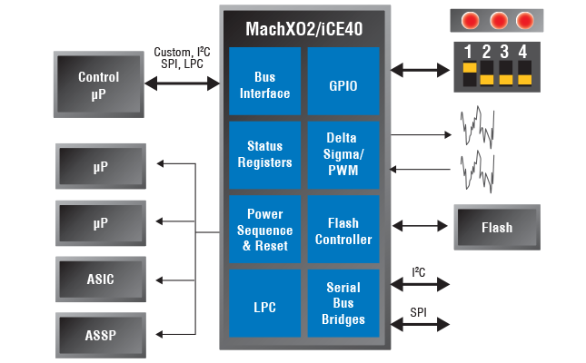
- Discover how the hardened dual I2C, SPI, and Timer/Counter functions augment the flexible I/Os and logic blocks in the MachXO2 to efficiently support MCU-based designs.
- See how a sensor monitoring solution example takes full advantage of the MachXO2 I/O expansion capabilities.
- Watch the 7-minute video to better understand how the MachXO2 efficiently integrates system functionality and how easy it is to get started with free design tools, IP trials and reference designs.
Visit the “Lattice MachXO2 I/O Expansion” web page to explore the full capabilities of the MachXO2 as an MCU I/O expansion device, or please
contact Allyanz todayfor more details.
LatticeECP3 Delivers Rock Solid SERDES for Low Cost PCIe 2.0 Designs
The LatticeECP3 PCIe Solution is the first and only PCI Express 2.0 compliant low cost FPGA. With rock solid SERDES, an advanced PCI Express IP Core and a full-featured development kit the LatticeECP3 solution is ready to accelerate your next PCIe innovation, with an affordable price tag.
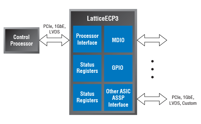
- With up to 16 channels of low cost, low power SERDES, DSP slices, high-speed DDR3 memory interface capability and efficient FPGA fabric, the LatticeECP3 has all the features required for PCIe applications.
- The Lattice PCI Express Endpoint IP Core has the advanced features needed to easily integrate PCIe 2.0 functionality with your design. Additionally, the Lattice Scatter Gather DMA IP Core can be used to further optimize transfer bandwidth.
- The LatticeECP3 Versa Development Kit includes the full-featured evaluation board (with LatticeECP3 FPGA, Flash and DDR3 memory), free Lattice Diamond design environment, reference designs, demonstration systems and complete user documentation.
Visit the “LatticeECP3 PCIe Information Page” to learn how to simplify your low cost PCIe applications, or please contact Allyanz today for more details.
Programmable Logic Devices Cuts Bill of Material Costs by up to 50%
Cut Bill of Material Costs by up to 50% for Board Power Management Functions
Programmable logic devices have been integrating digital functions to reduce cost, reduce board space and improve reliability for decades. Lattice’s programmable Power Manager II delivers these same capabilities, for both analog and digital functions, to dramatically cut bill of materials costs up to 50%, for board power management when compared to non-programmable implementations.
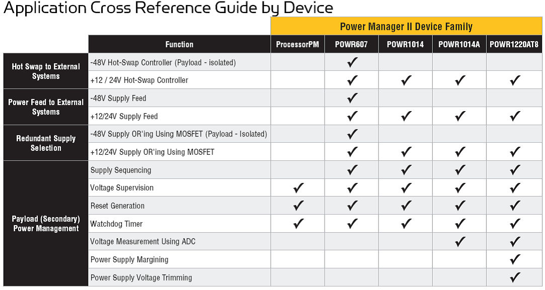
- Discover how the Power Manager II can easily integrate even advanced functions, like hot-swap control, power sequencing and reset generation with fast shutdown times and over a wide voltage range.
- See a design example that implements a hot-swap controller and manages the 1.2V, 2.5V and 3.3V board supply rails.
- Watch the video to see how the Power Manager II solves common system challenges associated with 12V hot swap designs.
Visit the “How Swap Controller using Power Manager II” web page to explore the full capabilities of the Power Manager II for Hot Swap Designs, or please contact Allyanz today for more details.
Lattice Semiconductor Announces Serial Image Sensor Bridge Support For Sony IMX136/104
Lattice Semiconductor Corporation (NASDAQ: LSCC), has announced the release of a serial sub-LVDS bridge design to support the Sony IMX136 and IMX104 image sensors. The serial sub-LVDS format is expected to become Sony’s primary image sensor interface for embedded/industrial users.
This new image sensor bridge design utilizes the low cost, low power Lattice MachXO2(tm) PLD (programmable logic device) to interface to the serial sub-LVDS bus of the Sony IMX136 or IMX104 image sensor. Applications that can benefit from this design include Surveillance cameras, Video conferencing and Industrial cameras.
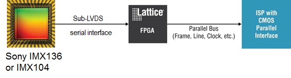
This image sensor bridge design allows an ISP (Image Signal Processor) with a CMOS parallel interface bus to connect to the Sony IMX136 or IMX104. The Lattice MachXO2-1200 device interfaces directly to the sub-LVDS I/Os and no external discrete components are required. The image sensor bridge application can support 1080P60 resolution with a 12-bit ISP interface.
If customers desire the full 1080P120 capability of the Sony IMX136 or IMX104, then the design code in the MachXO2 device can be modified easily to accommodate this. The image sensor bridge design is available now for download, and the MachXO2-1200 is in full production.
Key features:
- Complete Reference Designs in MachXO2-1200 or XP2-5
- Designed to Emulate Parallel Sensor Output Bus Width of 10 or 12 Bits
- Serial sub-LVDS interface to CMOS SDR data
- Legacy sub-LVDS parallel DDR to CMOS SDR also available
- Tested with Sony IMX036 and TI DM812X at 1080p60
- Converts the Sub-LVDS Sync Commands to Line Valid and Frame Valid Signals
- Bridge Device Offered in Space-saving 8×8 mm 132-Ball csBGA. TQFP Packages Also Available.
- Requires No External PROM
- Parallel Interface can be Configured for 1.8V, 2.5V or 3.3V LVCMOS Levels
To obtain the Sony IMX136 or IMX104 serial image sensor bridge design files, visit http://www.latticesemi.com/products/intellectualproperty/referencedesigns/sonyimx036sensorwithsublv.cfm , or please contact Allyanz.
Lattice Announces Production Release Of iCE40 “Los Angeles” LP-Series And HX-Series mobileFPGA Device Families
Two New iCEblink40 Development Kits Enable Access to Production-Qualified, Non-volatile 40nm Programmable Technology
Lattice Semiconductor Corporation (NASDAQ: LSCC) has announced that eight devices of its iCE40TM “Los Angeles” mobileFPGATM family have been fully qualified and released into volume production. The LP640, LP1K, LP4K and LP8K devices of the iCE40 low power LP-Series, and the HX640, HX1K, HX4K and HX8K devices of the higher performance iCE40 HX-Series, have been production released with 17 different device/package combinations.

The iCE40 mobileFPGA family, fabricated on non-volatile 40nm technology, follows the very successful 65nm iCE65TM family that has already been adopted by large consumer electronics OEMs who have taken advantage of its flexibility, low power, low cost and small footprint to quickly create new and innovative consumer products within ever shrinking development cycles.
Easy to Use Development Kits
With two new iCEblinkTM Development Kits, engineers can easily evaluate and adopt non-volatile iCE40 technology. The iCEblink40-HX (higher performance) Development Kit comes with an iCE40HX1K-VQ100 device and the iCEblink40-LP (low power) Development Kit comes with an iCE40LP1K-QN84 device. Both devices offer 1280 look up tables of logic, 64K bits of on-chip memory, and 67 user I/O. The USB-powered iCEblink40 Development Kits include features such as 1Mbit of SPI Flash memory, capacitive touch buttons, LEDs and access to all user I/O.
The iCEblink40 Development Kits are available for immediate purchase on Lattice’s website. For more information on the iCEblink40HX Development Kits, or the ultra low power consuming iCE40 mobileFPGAs, visit www.latticesemi.com/iCEblink40-HX1K, or please contact Allyanz.