Specialist Supplier Of Electronic Components, Semiconductors & Rugged Electronic Systems.

Allyanz Electronics, Semiconductors, Integrated Modules, Displays. Manufacturers Representative & Distributor Australia, NZ & South East Asia. Tel: +61.3.9759 5949

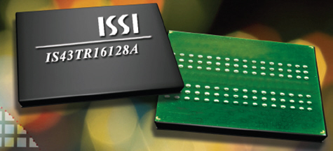
ISSI Now Offering UFS 2.1/2.2 - Universal Flash Storage

- Low-voltage supplies: 1.8V, 1.1V
- I/O at 1.1V (LPDDR4) or 0.6V (LPDDR4X)
- Clock Frequency Range : 10MHz to 2133MHz
- Data rates from : 20Mbps to 4266 Mbps per I/O
16n Pre-fetch DDR Architecture
- Multiplexed, double data rate, command/address inputs
- ZQ Calibration
- Mobile features for lower power
- Long-term, reliable support  

- Low-voltage supplies: 1.8V, 1.1V
- I/O at 1.1V (LPDDR4) or 0.6V (LPDDR4X)
- Clock Frequency Range : 10MHz to 2133MHz
- Data rates from : 20Mbps to 4266 Mbps per I/O
16n Pre-fetch DDR Architecture
- Multiplexed, double data rate, command/address inputs
- ZQ Calibration
- Mobile features for lower power
- Long-term, reliable support  

- Low-voltage supplies: 1.8V, 1.1V
- I/O at 1.1V (LPDDR4) or 0.6V (LPDDR4X)
- Clock Frequency Range : 10MHz to 2133MHz
- Data rates from : 20Mbps to 4266 Mbps per I/O
16n Pre-fetch DDR Architecture
- Multiplexed, double data rate, command/address inputs
- ZQ Calibration
- Mobile features for lower power
- Long-term, reliable support  

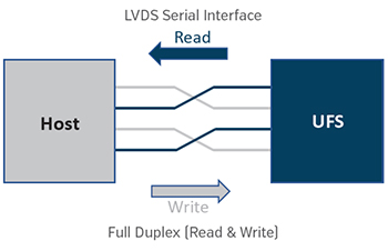
LVDS Serial Interface
ISSI Now Offering UFS 2.1/2.2 - Universal Flash Storage
previous arrow
next arrow
Shadow

Programmable Logic Devices Cuts Bill of Material Costs by up to 50%

Cut Bill of Material Costs by up to 50% for Board Power Management Functions
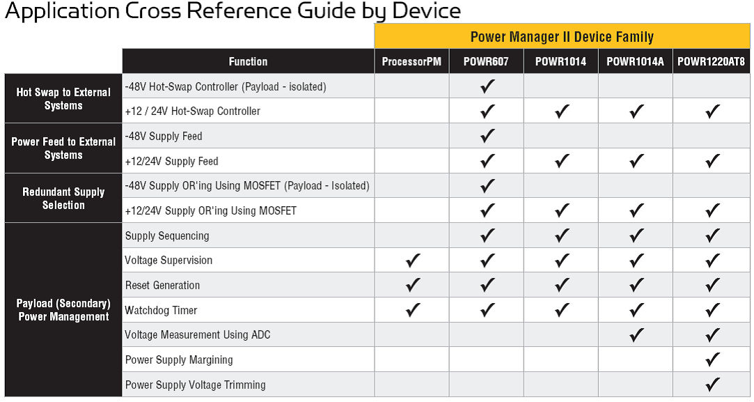
Programmable logic devices have been integrating digital functions to reduce cost, reduce board space and improve reliability for decades. Lattice’s programmable Power Manager II delivers these same capabilities, for both analog and digital functions, to dramatically cut bill of materials costs up to 50%, for board power management when compared to non-programmable implementations.


Board Power Management Functions

  • Discover how the Power Manager II can easily integrate even advanced functions, like hot-swap control, power sequencing and reset generation with fast shutdown times and over a wide voltage range.
  • See a design example that implements a hot-swap controller and manages the 1.2V, 2.5V and 3.3V board supply rails.
  • Watch the video to see how the Power Manager II solves common system challenges associated with 12V hot swap designs.

Visit the “How Swap Controller using Power Manager II” web page to explore the full capabilities of the Power Manager II for Hot Swap Designs, or please contact Allyanz today for more details.

Return to What’s New Page

ISSI Now Sampling 1Gbit & 2Gbit DDR3 DRAM

ISSI is now sampling its 1Gbit 1.5V DDR3 DRAM. Samples of the x16 data width option are now shipping (IS43TR16640A for Commercial and Industrial, or IS46TR16640A for Automotive). Samples of the x8 data width option will begin to ship soon (IS43TR81280A for Commercial and Industrial, or IS46TR81280A for Automotive).

ISSI NOW SAMPLING 1Gbit & 2Gbit DDR3 DRAM

The DDR3 interface is a popular interface for the latest microprocessors, ASICs, and ASPs. One of the advantages with DDR3 over predecessor technologies is the higher throughput: ISSI’s initial samples reach data rates of 1600 MT/s (800 MHz), with plans to support higher data rates in future.

ISSI DDR3 features include:

  • Bidirectional differential data strobe
  • Data masking per byte on Write commands
  • Programmable burst length of 4 or 8
  • Programmable CAS Latency
  • Auto-Refresh and Self-Refresh Modes
  • OCD (Driver Adjustment)
  • ODT (On Die Termination) supported
  • Write Leveling
  • Packages: 96-ball BGA for x16, 78-ball BGA for x8
  • Long-term support

“The expansion of broadband infrastructure in data centers and customer-premise equipment are driving system designers to incorporate DDR3 DRAMs into their products. These applications also have long-life requirements, so ISSI’s commitment to long-term support of the 1Gbit and 2Gbit DDR3 products will be important for our customers in the communications and networking markets,” said Ron Kalakuntla, vice president of marketing at ISSI. Key applications are Automotive multimedia, navigation and clusters, along with the communications market segment, which includes access and aggregation nodes, routers and switches, network storage, optical transport and base stations.

Please contact Allyanz today to place your sample order.

Return to What’s New Page

Lattice Semiconductor Announces Serial Image Sensor Bridge Support For Sony IMX136/104

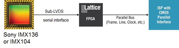
Lattice Semiconductor Corporation (NASDAQ: LSCC), has announced the release of a serial sub-LVDS bridge design to support the Sony IMX136 and IMX104 image sensors. The serial sub-LVDS format is expected to become Sony’s primary image sensor interface for embedded/industrial users.

This new image sensor bridge design utilizes the low cost, low power Lattice MachXO2(tm) PLD (programmable logic device) to interface to the serial sub-LVDS bus of the Sony IMX136 or IMX104 image sensor. Applications that can benefit from this design include Surveillance cameras, Video conferencing and Industrial cameras.

Lattice Semiconductor Announces Serial Image Sensor Bridge Support For Sony IMX136/104

This image sensor bridge design allows an ISP (Image Signal Processor) with a CMOS parallel interface bus to connect to the Sony IMX136 or IMX104. The Lattice MachXO2-1200 device interfaces directly to the sub-LVDS I/Os and no external discrete components are required. The image sensor bridge application can support 1080P60 resolution with a 12-bit ISP interface.

If customers desire the full 1080P120 capability of the Sony IMX136 or IMX104, then the design code in the MachXO2 device can be modified easily to accommodate this. The image sensor bridge design is available now for download, and the MachXO2-1200 is in full production.

Key features:

  • Complete Reference Designs in MachXO2-1200 or XP2-5
  • Designed to Emulate Parallel Sensor Output Bus Width of 10 or 12 Bits
  • Serial sub-LVDS interface to CMOS SDR data
  • Legacy sub-LVDS parallel DDR to CMOS SDR also available
  • Tested with Sony IMX036 and TI DM812X at 1080p60
  • Converts the Sub-LVDS Sync Commands to Line Valid and Frame Valid Signals
  • Bridge Device Offered in Space-saving 8×8 mm 132-Ball csBGA. TQFP Packages Also Available.
  • Requires No External PROM
  • Parallel Interface can be Configured for 1.8V, 2.5V or 3.3V LVCMOS Levels

To obtain the Sony IMX136 or IMX104 serial image sensor bridge design files, visit http://www.latticesemi.com/products/intellectualproperty/referencedesigns/sonyimx036sensorwithsublv.cfm , or please contact Allyanz.

Return to What’s New Page

ISSI supporting 2Gb DDR2 SDRAM

Targeted for Automotive, Communications, Medical, and Industrial Applications

Integrated Silicon Solution, Inc. (Nasdaq:ISSI), a leader in advanced memory solutions, is now supporting volume production units of its new 2 Gigabit (2Gb) DDR2 device, the newest addition to ISSI’s family of DDR2 SDRAMs.

The first device is the IS43DR16128, which is organized as 128Mx16 and packaged in an 84-ball BGA. This on-going expansion of the DDR2 SDRAM product family adds to ISSI’s extensive offering of DRAM.

By using advanced technology, ISSI is able to provide the long-term product support required by long lifecycle applications in automotive, communications, medical, and industrial designs.

The new device is available with clock speeds up to 333MHz (DDR2-667).

In addition to this 2Gb DDR2 DRAM, ISSI also offers 1Gb, 512Mb and 256Mb DDR2 devices in commercial, industrial, and automotive temperature grades.

The 256Mb density includes x32, x16, and x8 organizations, while the 512Mb and 1Gb densities include x16 and x8 organizations. The DDR2 DRAM product family operates from a single supply voltage of 1.8V.

“Our automotive customers are excited by our expanding portfolio of high-density DRAMs and our long-term commitment. Customers have begun to qualify the new 2Gb DDR2 device in vehicle infotainment systems, where the integration of new features is driving memory demand,” said Lyn Zastrow, vice president of the Automotive Business Unit at ISSI.

“The mobile data explosion is driving memory density requirements in mobile infrastructure products, such as base stations. Additionally these applications have long-life requirements, so long-term support of 2Gb DDR2 products is key for our customers in that space,” said Pat Lasserre, director of the Communications Business Unit at ISSI. Key applications in communications include access and aggregation nodes, routers and switches, network storage, optical transport, and base stations. Other applications include medical instrumentation, energy meters, and security systems.

In addition to SDR, mobile SDR/DDR, DDR, and DDR2 SDRAMs, ISSI also offers a complete line of both asynchronous and synchronous SRAM with densities from 64Kb to 72Mb. ISSI also has a range of SPI (NOR) Flash, and Known Good Die (KGD) memories in its portfolio.

For more details on ISSI’s range of DDR2 DRAM, including datasheets, samples or pricing, please contact Allyanz.

Return to What’s New Page

Lattice Announces Production Release Of iCE40 “Los Angeles” LP-Series And HX-Series mobileFPGA Device Families

Two New iCEblink40 Development Kits Enable Access to Production-Qualified, Non-volatile 40nm Programmable Technology

Lattice Semiconductor Corporation (NASDAQ: LSCC) has announced that eight devices of its iCE40TM “Los Angeles” mobileFPGATM family have been fully qualified and released into volume production. The LP640, LP1K, LP4K and LP8K devices of the iCE40 low power LP-Series, and the HX640, HX1K, HX4K and HX8K devices of the higher performance iCE40 HX-Series, have been production released with 17 different device/package combinations.

Lattice Semiconductor iCE40 mobileFPGA family

The iCE40 mobileFPGA family, fabricated on non-volatile 40nm technology, follows the very successful 65nm iCE65TM family that has already been adopted by large consumer electronics OEMs who have taken advantage of its flexibility, low power, low cost and small footprint to quickly create new and innovative consumer products within ever shrinking development cycles.

Easy to Use Development Kits

With two new iCEblinkTM Development Kits, engineers can easily evaluate and adopt non-volatile iCE40 technology. The iCEblink40-HX (higher performance) Development Kit comes with an iCE40HX1K-VQ100 device and the iCEblink40-LP (low power) Development Kit comes with an iCE40LP1K-QN84 device. Both devices offer 1280 look up tables of logic, 64K bits of on-chip memory, and 67 user I/O. The USB-powered iCEblink40 Development Kits include features such as 1Mbit of SPI Flash memory, capacitive touch buttons, LEDs and access to all user I/O.

The iCEblink40 Development Kits are available for immediate purchase on Lattice’s website. For more information on the iCEblink40HX Development Kits, or the ultra low power consuming iCE40 mobileFPGAs, visit www.latticesemi.com/iCEblink40-HX1K, or please contact Allyanz.

Return to What’s New Page
Archives