Specialist Supplier Of Electronic Components, Semiconductors & Rugged Electronic Systems.

Allyanz Electronics, Semiconductors, Integrated Modules, Displays. Manufacturers Representative & Distributor Australia, NZ & South East Asia. Tel: +61.3.9759 5949

ISSI Now Offering UFS 2.1/2.2 - Universal Flash Storage

- Low-voltage supplies: 1.8V, 1.1V
- I/O at 1.1V (LPDDR4) or 0.6V (LPDDR4X)
- Clock Frequency Range : 10MHz to 2133MHz
- Data rates from : 20Mbps to 4266 Mbps per I/O
16n Pre-fetch DDR Architecture
- Multiplexed, double data rate, command/address inputs
- ZQ Calibration
- Mobile features for lower power
- Long-term, reliable support  

- Low-voltage supplies: 1.8V, 1.1V
- I/O at 1.1V (LPDDR4) or 0.6V (LPDDR4X)
- Clock Frequency Range : 10MHz to 2133MHz
- Data rates from : 20Mbps to 4266 Mbps per I/O
16n Pre-fetch DDR Architecture
- Multiplexed, double data rate, command/address inputs
- ZQ Calibration
- Mobile features for lower power
- Long-term, reliable support  

- Low-voltage supplies: 1.8V, 1.1V
- I/O at 1.1V (LPDDR4) or 0.6V (LPDDR4X)
- Clock Frequency Range : 10MHz to 2133MHz
- Data rates from : 20Mbps to 4266 Mbps per I/O
16n Pre-fetch DDR Architecture
- Multiplexed, double data rate, command/address inputs
- ZQ Calibration
- Mobile features for lower power
- Long-term, reliable support  

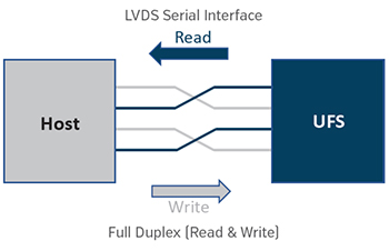
LVDS Serial Interface
ISSI Now Offering UFS 2.1/2.2 - Universal Flash Storage
previous arrow
next arrow
Shadow

ISSI Releases 1 Gb High Speed DDR2 SDRAM for Automotive, Networking, Telecommunications, and Industrial Applications

ISSI, a leader in advanced memory solutions, has added the 1 Gigabit density to their family of DDR2 SDRAMs. The first device at this new density is the IS43DR16640A which is organized as 64Mx16 and packaged in an 84-ball BGA. This on-going expansion of the DDR2 SDRAM product family adds to ISSI’s already extensive offering of DRAM devices.

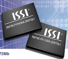
ISSI 400MHz - 72 MB Synchronous SRAM

This new device is available with clock speeds up to 533MHz (DDR2-1066), providing a data transfer rate of 4 gigabytes/sec in 32 bit systems. In addition to this new 1Gb device, ISSI also offers 512Mb and 256Mb DDR2 devices, with all three densities available in commercial, industrial and automotive grades. The 256Mb density includes 8Mx32 and 16Mx16 organizations and for the 512Mb density 32Mx16 and 64Mx8 organizations are available. ISSI plans to release x8 bit wide configurations of the 256Mb, and 1Gb devices later in 2010. The DDR2 DRAM product family from ISSI operates from a single 1.8V supply voltage.

For more details on the 1Gb DDR2 SDRAM, or other SRAM or DRAM devices from ISSI, please contact us.

Return to What’s New Page

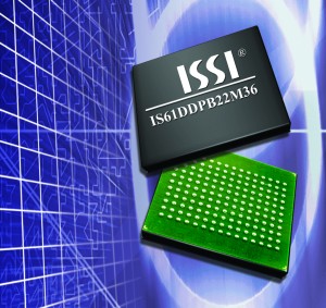
ISSI SHIPPING 400Mhz, 72Mb Synchronous SRAM

ISSI is now sampling its 72Mb IS61DDPB22M36 and IS61DDPB24M18 synchronous, high-performance CMOS SRAM devices. These SRAMs are available in 18 & 36 bit configurations, with a Double Data Rate (DDR-IIP) interface for read and write input ports.

72Mb IS61DDPB22M36

Other features these DDR-IIP Synchronous SRAM offer include:

  • On-chip delay-locked loop (DLL) for wide data valid window.
  • Common data input/output bus.
  • Synchronous pipeline read with self-timed late write operation.
  • Fixed 2-bit burst for read and write operations.
  • Clock stop support.
  • Two input clocks (K and K) for address and control registering at rising edges only.

The devices are available in commercial & industrial temperature ranges.
For more details on these high density, high performance DDR-IIP Synchronous SRAM from ISSI, please contact us.

For more details about DDR-IIP Synchronous SRAM, please contact us.

Return to What’s New Page

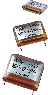
WIMA RFI Capacitors with High Corona Inception Voltag

WIMA RFI Capacitors with High Corona Inception Voltage

The MKP-X2 R series capacitors from WIMA are suited to demanding AC voltage circuits e.g. where voltage is supplied via a capacitor power supply (the capacitor is switched in series to the load circuit as a low-loss series impedance). Due to their internal series connection the capacitors exhibit about twice as high corona inception voltage, resulting in higher rated AC voltage values than comparable components without this series connection.

WIMA MKP-X2 R capacitors are available with extended capacitance values up to 10 microF and a rated voltage of 400 VAC.

For more details on the MKP-X2 R series of RFI capacitors from WIMA, please contact us.

Return to What’s New Page

Lattice Releases Development Platform for SERDES and Video Clock Distribution

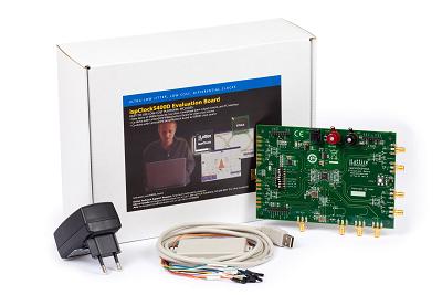
lattice-5400d_eval_board_al

Lattice Semiconductor is now shipping its US$169 evaluation board for the ispClockTM 5400D programmable clock device.

The new board is an easy-to-use platform for evaluating and designing with the ispClock5400D differential clock distribution device. The evaluation board can be used by itself to review the performance and in-system programmability of the 5400D device, or as a companion board and clock source for LatticeECP3TM FPGA Serial Protocol or Video Protocol evaluation boards.

Typically, expensive oscillators with LVDS or LVPECL interfaces are used as a reference clock for FPGA SERDES interface applications. The ispClock5400D device provides ultra low-jitter differential clock outputs that can be used to drive both the general purpose clocks and the SERDES reference clocks for FPGAs, ASSPs and ASICs. The evaluation board demonstrates how to interface a low-cost CMOS interface oscillator to the ispClock5400D device to produce high quality clocks for XAUI applications or 270 MHz SDI video applications.

About ispClock Programmable Clock Devices

The ispClock5400D device family features in-system programmable differential clock distribution with fully programmable features that allow users to program in different frequencies based on dividers and PLL functions. Additional value is added with multiple differential I/O support for various standards while maintaining the low-jitter required for high performance systems. The ispClock5400D family supports differential output drivers for programmable differential input reference/feedback standards: LVDS, LVPECL, HSTL, SSTL and HCSL. Included on-chip are programmable termination and a clock A/B selection multiplexer, programmable time skew, programmable phase skew and various programmable output enable features. Through I2C the user has access to nearly all the programmable features of the ispClock5400D.

The ispClock5400D maintains extremely low-jitter:

  • Ultra low cycle-to-cycle jitter (29ps p-p)
  • Ultra low period jitter (2.5ps)
  • Low output-to-output skew (<75ps)

About LatticeECP3 FPGAs

The low power, high value, third generation LatticeECP3 family offers the industry’s lowest power consumption and price of any SERDES-capable FPGA devices.The LatticeECP3 FPGA family offers multi-protocol 3.2G SERDES with XAUI jitter compliance, DDR3 memory interfaces, powerful DSP capabilities, high density on-chip memory and up to 149K LUTS, all with half the power consumption and half the price of competitive SERDES-capable FPGAs.

For more details on the low cost Evaluation board, ispClock5400D devices or ECP3 SERDES-capable FPGAs, please contact us.

Return to What’s New Page

Single Chip, Non-Volatile LatticeXP2 FPGA

lattice_single_chip-non-volatile_latticexp2_fpgas

Lattice Semiconductor is now shipping industrial temperature, and automotive temperature (AEC-Q100, with PPAP support) qualified versions of its non-volatile LatticeXP2(TM) FPGAs in volume production quantities. Based on Lattice’s 90 nanometer hybrid flexiFLASH(TM) technology, the XP2 family’s volume production availability enables realization of design requirements in a multitude of industrial applications such as medical imaging, robotics, human machine interface (HMI) systems, motor control and industrial displays, as well as in the tightest form-factor automotive applications such as automotive camera modules, telematics systems, parking assistance systems and multimedia systems.

The non-volatile LatticeXP2 FPGA family is a compelling solution for designers who value single chip integration, impressive processing power in the smallest footprint, source synchronous interfaces, design security and low power consumption. The XP2 FPGAs unique benefits include low cost, small form factor Chip Scale 132 BGA packaging, and increased functionality such as embedded sysDSP(TM) blocks, pre-engineered source-synchronous I/O that supports 7:1 LVDS, DDR2 and high-speed ADCs/DACs.

Unlike traditional SRAM-based FPGAs, the LatticeXP2 device does not require an external boot memory for FPGA configuration, which enables a single-chip solution with the associated benefits of reduced board area and simplified system manufacture. The absence of an external boot device also eliminates the need for an external bit-stream at boot up and the possibility of bit-stream snooping, a major security concern with SRAM FPGAs. Additional security features prohibit bit-stream readback from the SRAM and Flash sections of the devices.

The LatticeXP2 design solution offers a unique set of features with broad appeal to a variety of markets, such as video security/ surveillance, LCD/display controllers, automotive systems, medical imaging, and industrial control systems, where processing power must be delivered with high integration in low-cost, small footprint packaging.

About flexiFLASH Architecture
xp2_system_diagram_small

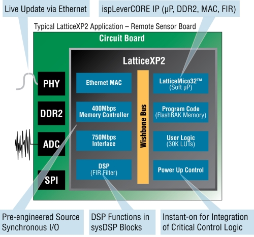
Flash memory blocks are embedded within XP2 FPGAs to store the device configuration, providing a true single chip solution. At power up or on user command, the data stored in the Flash memory is transferred into SRAM cells that control the configuration of the device. This transfer is done in a massively parallel fashion, enabling the device logic to be available in under 1mS, well ahead of the other devices in the system and much faster than SRAM-based FPGAs that use external boot PROMs, regardless of whether they are provisioned separately on-board or stacked in the same package. This instant-on capability is critical for many system functions such as power up sequencing, address decoding and reset logic.

For more details on the single chip, non-volatile LatticeXP2(TM) FPGAs, or development tools to support your design requirements, please contact us.

Return to What’s New Page

Archives