ISSI is currently sampling 64 GB, 128 GB & 256 GB devices, supporting UFS 2.1, and UFS 2.2. ISSI’s UFS product family provides the ideal embedded storage solution for the Automotive, Industrial, Medical, Networking, and Consumer applications, which require high performance, endurance, and low power across a wide range of operating temperatures, with long-term support.
ISSI is currently sampling 64 GB, 128 GB & 256 GB devices, supporting UFS 2.1, and UFS 2.2. ISSI’s UFS product family provides the ideal embedded storage solution for the Automotive, Industrial, Medical, Networking, and Consumer applications, which require high performance, endurance, and low power across a wide range of operating temperatures, with long-term support.
ISSI is currently sampling 64 GB, 128 GB & 256 GB devices, supporting UFS 2.1, and UFS 2.2. ISSI’s UFS product family provides the ideal embedded storage solution for the Automotive, Industrial, Medical, Networking, and Consumer applications, which require high performance, endurance, and low power across a wide range of operating temperatures, with long-term support.
ISSI’s SLC NAND Flash devices support a wide operating temperature range of -40C to 105C, making them ideal for next generation automotive, industrial and Internet of Things (IoT) applications. Both the SPI NAND and parallel NAND Flash devices are AEC-Q100 qualified meeting the stringent automotive qualification requirements. ISSI offers parallel SLC NAND in 1Gb, 2Gb, 4Gb & 8Gb densities.
ISSI’s SLC NAND Flash devices support a wide operating temperature range of -40C to 105C, making them ideal for next generation automotive, industrial and Internet of Things (IoT) applications. Both the SPI NAND and parallel NAND Flash devices are AEC-Q100 qualified meeting the stringent automotive qualification requirements. ISSI offers parallel SLC NAND in 1Gb, 2Gb, 4Gb & 8Gb densities.
ISSI’s SLC NAND Flash devices support a wide operating temperature range of -40C to 105C, making them ideal for next generation automotive, industrial and Internet of Things (IoT) applications. Both the SPI NAND and parallel NAND Flash devices are AEC-Q100 qualified meeting the stringent automotive qualification requirements. ISSI offers parallel SLC NAND in 1Gb, 2Gb, 4Gb & 8Gb densities.

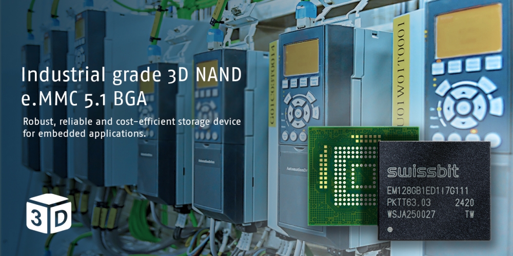
Swissbit, a leading manufacturer of flash memory solutions, presents its latest technology for demanding industrial, medical & automotive markets: eMMC memory, EM-30.
Swissbit, a leading manufacturer of flash memory solutions, presents its latest technology for demanding industrial, medical & automotive markets: eMMC memory, EM-30.
Integrated Silicon Solution, Inc. (ISSI), a leader in advanced memory and analog solutions, has begun sampling production units of automotive grade 512Mb Serial (SPI) NOR Flash.
Integrated Silicon Solution, Inc. (ISSI), a leader in advanced memory and analog solutions, has begun sampling production units of automotive grade 512Mb Serial (SPI) NOR Flash.

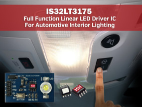
ISSI Full Function LED Driver IC For Automotive Interior Lighting. Integrated Silicon Solution, Inc. (ISSI), a leader in advanced memory and analog IC solutions, has announced a single chip solution for automotive interior lighting.